The Mask Gets Larger
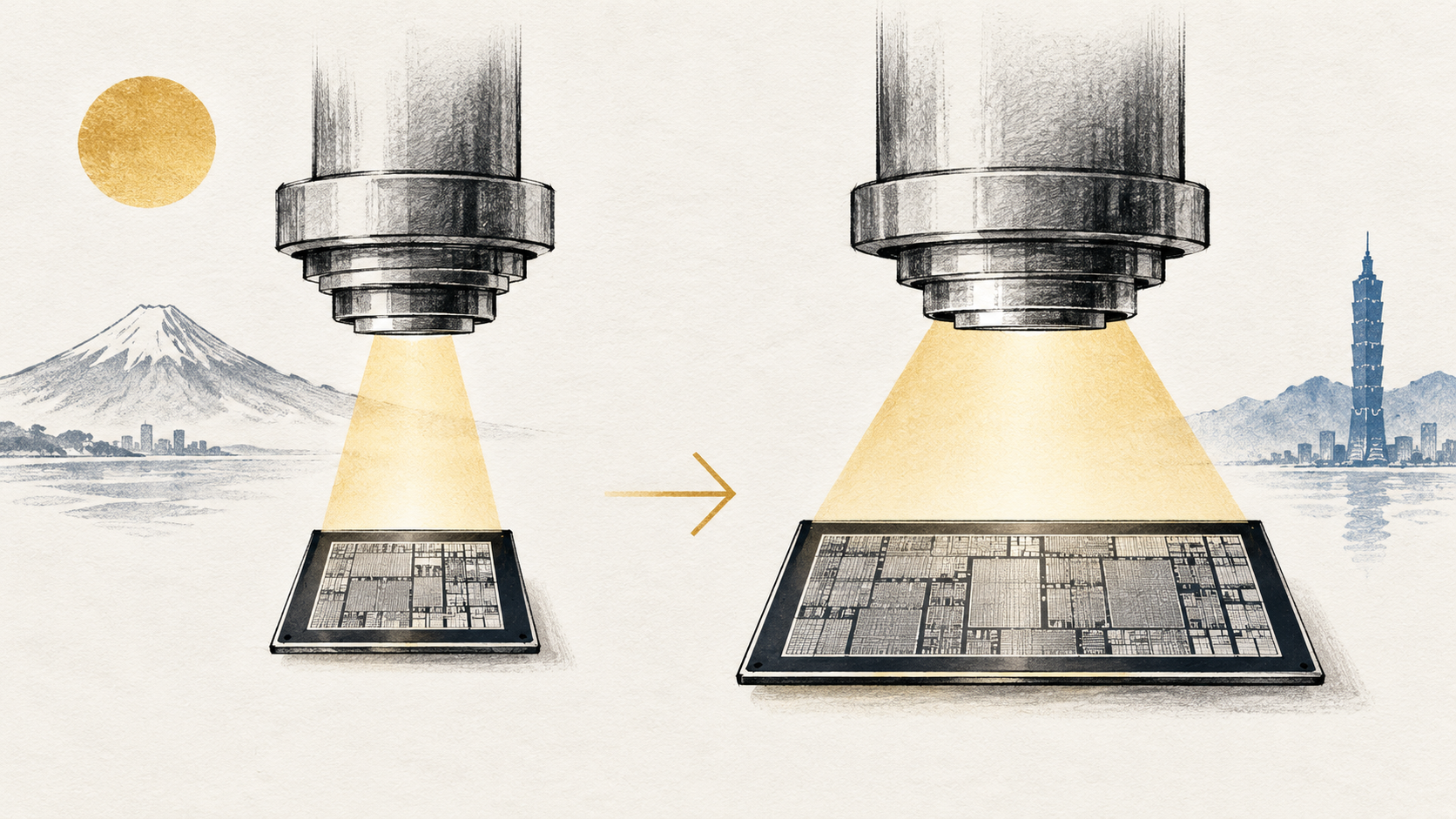
To keep transistors shrinking, AI is forcing the semiconductor system around them to grow.
For decades, the semiconductor industry followed a remarkably simple direction. Chips became more powerful because manufacturers learned to print ever smaller structures onto silicon, while much of the infrastructure surrounding that process remained relatively stable. That balance is beginning to change.
ASML and TSMC are working with semiconductor companies including Samsung and Intel on a larger photomask format for the next generation of High-NA EUV lithography. TSMC expects to introduce High-NA into advanced chip production around 2030, while the larger-mask platform is being developed for the years that follow.
At first sight, changing the size of a mask sounds like a highly specialised manufacturing adjustment. But it raises a much larger question: Why does making chips smaller suddenly require parts of the semiconductor factory to become larger?
🟧 01 | Why does High-NA need a larger mask?
High-NA EUV allows manufacturers to print even smaller structures on advanced chips. But the new optical system comes with a trade-off: the area that can be exposed at once becomes smaller when today’s mask format is used. That matters because many advanced processors, particularly those used for AI, are physically large.
A larger photomask would allow manufacturers to expose a larger area more efficiently and reduce the need to divide complex chip designs across separate exposures. The paradox is striking.
The technology designed to make transistors smaller is creating pressure to make part of the manufacturing system larger. And AI is one of the main reasons that pressure is becoming urgent.
🟧 02 | Why is AI changing the equation?
AI chips do not simply contain more computing power. They are increasingly large, complex systems designed to move enormous amounts of data between processors and memory. That creates a different challenge from traditional semiconductor scaling.
Manufacturers still want smaller transistors, but the chips built from them are not necessarily becoming smaller themselves. Advanced packaging and chiplets can divide some of that complexity across multiple pieces of silicon. Yet the demand for very large, highly integrated processors remains.
AI is therefore beginning to shape not only which chips are produced, but also how semiconductor factories must be designed to produce them. That makes the move toward larger masks more than an ASML engineering project. It becomes a supply-chain question.
🟧 03 | Which Asian players matter?
The centre of advanced semiconductor manufacturing remains firmly anchored in East Asia. TSMC in Taiwan is the world’s most important advanced logic manufacturer and intends to bring High-NA into high-volume production around 2030.
Samsung in South Korea is pursuing the technology across both advanced logic and memory, while SK Hynix is another important player as AI drives extraordinary demand for high-performance memory. Japan provides another, less visible layer.
Companies such as HOYA and AGC supply critical materials used in advanced photomasks. Lasertec occupies an important position in mask inspection, while Tekscend Photomask represents Japan’s specialist manufacturing capability in the mask itself. The importance of the initiative therefore lies partly in its geography.
Taiwan manufactures the leading logic. Korea supplies much of the advanced memory. Japan provides critical materials and equipment. But the lithography technology connecting those systems comes from Europe. Which puts ASML in an unusual position.
🟧 04 | What is ASML’s role?
ASML is usually described as a semiconductor-equipment manufacturer. That description is becoming increasingly incomplete.
A new generation of lithography cannot simply be delivered to a factory and switched on. Changes in the optical system affect masks, inspection equipment, materials, factory workflows and eventually the design choices made by chip manufacturers themselves. When ASML changes an important element of lithography, parts of the wider semiconductor ecosystem have to adapt around it.
TSMC, Samsung and Intel remain responsible for their own manufacturing strategies. Japanese suppliers retain control over specialised technologies within the mask ecosystem. But increasingly, those roadmaps intersect at one technological point.
ASML does not control the semiconductor industry. It does, however, provide one of the architectures around which the industry must coordinate. And coordination alone is not enough. The new system must also make economic sense.
🟧 05 | Why does the larger mask matter economically?
High-NA machines are among the most expensive pieces of manufacturing equipment ever installed in semiconductor fabs. That means better resolution alone cannot justify them. Chipmakers need the machines to operate efficiently enough to produce enormous volumes of chips at acceptable cost.
If very large processors require additional exposures or more complicated production steps, some of the benefit of the new lithography system disappears. A larger mask is intended to reduce that problem. This makes the change important for a reason that is easy to overlook.
The larger mask is not only about what High-NA can print. It is about whether High-NA can become economical enough to use at industrial scale. And once that question is considered, the significance of the initiative becomes much broader.
🟧 06 | What does this tell us about the next semiconductor era?
For much of semiconductor history, progress could be summarised in one phrase: make things smaller. That is no longer enough. Transistors are still shrinking, but AI is making processors larger and placing extraordinary demands on memory, packaging, energy and cooling. Now even parts of the lithography infrastructure are being reconsidered.
The proposed larger photomask is therefore interesting precisely because it appears to be such a small technical change. It shows that the semiconductor industry can no longer advance simply by improving one machine or shrinking one component. The system around the chip must evolve with it.
ALTAIR SIGNAL
The semiconductor roadmap is beginning to move in two directions at once. The transistor continues to shrink. The infrastructure required to turn those transistors into useful computing systems is becoming larger, more complex and more interconnected.
The new photomask captures that reversal in unusually physical form. And its geography reveals something equally important.
Dutch lithography, Taiwanese logic, Korean memory and Japanese materials are not separate semiconductor stories anymore. They are increasingly parts of the same production architecture.
AI may be designed in code. But its next generation will depend on whether an entire industrial system can scale with it.
Credit
Illustration: Altair Media Asia / OpenAI
Caption
Smaller transistors, larger infrastructure. The move toward larger photomasks shows how AI is beginning to reshape not only chip design, but the physical architecture of semiconductor manufacturing.
