SK Siltron: Where the Semiconductor Industry Begins
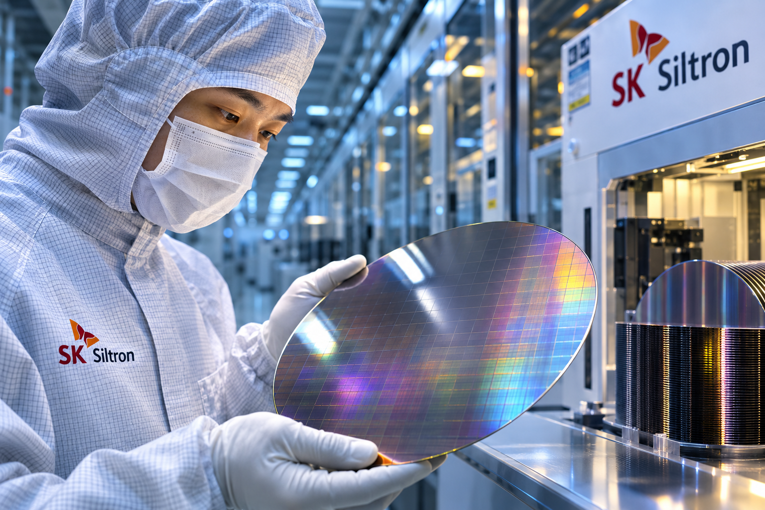
Before the world’s most advanced chips can be manufactured, someone must create the extraordinary material on which they are built.
The semiconductor revolution begins long before the first transistor is made. Before artificial intelligence can process information, before advanced memory can store it and before a processor can execute billions of calculations, something far less spectacular must happen. A manufacturer must create a nearly flawless surface on which the entire electronic architecture can be constructed.
That surface is a silicon wafer. A thin, circular disc with a mirror-like finish, it appears almost deceptively simple. Yet producing one requires extraordinary control over materials, temperature, crystal structure and microscopic imperfections. The smallest irregularities can influence processes that eventually determine whether billions of transistors function as intended.
The semiconductor revolution begins not with intelligence, but with the physical conditions that make intelligence possible.
Altair Media
Editorial analysis
South Korea’s SK Siltron operates at this largely invisible beginning of the semiconductor industry.
While companies such as Nvidia, TSMC and ASML attract global attention, wafer manufacturers occupy an earlier position in the industrial chain. Their contribution is rarely visible in the finished product, but without the materials they produce, the modern semiconductor industry could not operate.
The distinction is fundamental. Semiconductor innovation is not simply about designing smaller transistors or manufacturing more powerful processors. It begins with creating the physical conditions that make those achievements possible.
Turning Silicon into Precision
Silicon is one of the most abundant elements in the Earth’s crust. High-quality semiconductor wafers, however, are anything but ordinary.
The journey from raw material to semiconductor substrate involves a series of demanding industrial processes. Semiconductor-grade silicon can reach purity levels of 99.9999999% or higher—a degree of refinement that illustrates the extraordinary demands of modern chip manufacturing.
The purified silicon is melted and carefully transformed into a single crystal, typically through a method known as the Czochralski process. A seed crystal is slowly drawn from the molten material, allowing a cylindrical ingot to grow under precisely controlled conditions.
That ingot is then sliced into thin discs. Each wafer undergoes grinding, polishing, cleaning and inspection before it can be delivered to a semiconductor fabrication plant.
The objective is not merely to create a smooth surface. It is to produce a material whose geometry, purity and electrical characteristics meet tightly controlled specifications across the entire disc.
Modern semiconductor manufacturing commonly uses 300-millimetre silicon wafers. These provide the foundation for many of the world’s advanced logic and memory chips, allowing manufacturers to process numerous integrated circuits simultaneously.
The larger the wafer, the more demanding the requirements for uniformity become. A surface may appear perfectly flat to the human eye while containing variations significant enough to interfere with processes operating at nanometre scales.
For SK Siltron, precision is therefore not a final inspection requirement. It is the product itself.
The Economics of Imperfection
In semiconductor manufacturing, microscopic defects can carry enormous economic consequences.
A modern fabrication plant represents an investment of billions of dollars. Its profitability depends partly on how many functional chips emerge from each production cycle, a measure commonly described as manufacturing yield.
Wafer quality is one of the many factors influencing that outcome. Crystal defects, contamination, surface irregularities and variations in electrical properties can create difficulties during subsequent manufacturing stages. Not every imperfection results in a defective chip, and yield also depends on circuit design, process technology and manufacturing control. Nevertheless, the quality of the starting material establishes important limits on what follows.
This gives wafer manufacturing an economic significance that extends well beyond the price of a silicon disc. A reliable substrate helps manufacturers operate complex production processes with greater consistency, reducing uncertainty and contributing to more predictable manufacturing performance.
For semiconductor companies operating expensive fabrication facilities, that predictability has considerable value.
A silicon wafer is not simply a raw material. Its quality helps determine how efficiently billions of dollars in manufacturing capacity can be used.
Altair Media
Editorial analysis
The relationship also explains why wafer suppliers cannot easily be replaced. Qualification takes time, as customers must establish that a supplier’s materials behave consistently across highly sensitive manufacturing processes. Once those relationships are established, switching suppliers can introduce technical and commercial risks.
The competitive advantage is therefore built not only on the ability to manufacture wafers, but also on the ability to reproduce exceptional quality, shipment after shipment.
An Industry Few Companies Can Enter
The global silicon wafer industry is dominated by a remarkably small number of specialised manufacturers.
Japan’s Shin-Etsu Chemical and SUMCO, Taiwan’s GlobalWafers, Germany’s Siltronic and South Korea’s SK Siltron form the core of this highly concentrated market. Together, these five companies account for more than 90% of the global silicon wafer market by revenue, according to industry estimates, although market shares vary by wafer diameter and product category. Their position reflects formidable barriers to entry.
Building a wafer manufacturing facility requires substantial capital. Developing the necessary materials expertise takes years, while establishing reliable production at scale demands sophisticated equipment, extensive quality control and close relationships with semiconductor manufacturers.
Technical capability alone is insufficient. A supplier must demonstrate that its wafers perform consistently under the demanding conditions of industrial chip production. Qualification can take considerable time, making established customer relationships particularly valuable.
This combination of capital, accumulated knowledge and customer qualification creates an industry that is exceptionally difficult to enter.
It also reveals an important contrast with the more visible parts of the technology sector. Software companies can sometimes scale rapidly with relatively limited physical infrastructure. Wafer manufacturers depend on factories, equipment, engineering expertise and painstaking improvements in production processes.
Industrial leadership here is measured in consistency rather than spectacle.
Beyond Silicon: The Promise and Limits of Silicon Carbide
For decades, conventional silicon has provided the foundation for most semiconductor manufacturing. Yet not every electronic application benefits from the same material.
Power electronics, particularly systems operating at high voltages or temperatures, have created opportunities for alternatives such as silicon carbide, commonly known as SiC.
Silicon carbide possesses material properties that can enable more efficient power conversion under demanding operating conditions. This makes it attractive for applications including electric vehicles, industrial drives, charging infrastructure and certain energy systems.
SK Siltron expanded into this field through its American silicon carbide activities, seeking to establish a position in a market expected to benefit from electrification. The strategy reflected a broader industrial belief that electric mobility and energy transformation would generate sustained demand for advanced power semiconductors. But technological potential and commercial success do not always develop at the same pace.
The silicon carbide market has experienced pressure from uneven electric vehicle demand, changing investment expectations and expanding production capacity. Reports in 2026 indicated that SK Siltron was moving to wind down its American silicon carbide operations following financial difficulties.
The contrast is instructive. A material may offer compelling technical advantages without immediately supporting a commercially sustainable manufacturing business.
New semiconductor technologies require more than scientific validation. They need customers, production volumes, competitive costs and a market prepared to absorb industrial capacity.
A technological breakthrough does not automatically create an industrial success. Between invention and profitability lies the challenge of scale.
Altair Media
Editorial analysis
The experience reveals a fundamental distinction between innovation and industrialisation. Developing an advanced material is one achievement. Building a profitable global supply business around it is another.
A New Chapter in South Korea’s Industrial Architecture
SK Siltron’s strategic importance extends beyond its factories. For years, the company formed part of South Korea’s SK industrial group, whose activities span semiconductors, energy, telecommunications and advanced materials.
In July 2026, Doosan announced an agreement to acquire a controlling interest of approximately 70.6% in SK Siltron, marking a potentially significant change in the ownership of one of the country’s important semiconductor materials businesses. Completion was envisaged for early 2027, subject to the relevant conditions.
The proposed transaction reflects a broader industrial logic. Doosan has been expanding its involvement in advanced electronic materials and semiconductor-related industries. Bringing a major wafer producer into that portfolio could create opportunities to combine manufacturing capabilities, customer relationships and materials expertise.
Yet ownership changes also introduce questions about future priorities.
Will the new industrial structure accelerate investment in conventional silicon wafers? Will it change the balance between technological development and financial discipline? And how will SK Siltron position itself as the semiconductor industry expands production capacity across Asia, Europe and North America?
These questions matter because semiconductor materials are not easily relocated or rapidly expanded. Their industrial value rests on continuity, long-term investment and the confidence of customers whose own production processes depend on reliable supply.
The future of SK Siltron will therefore be shaped not only by technological demand, but also by the strategic priorities of its owners.
The Material Foundation of Artificial Intelligence
Artificial intelligence has transformed the global semiconductor conversation.
Much of the attention focuses on graphics processors, advanced memory and the enormous computing facilities required to train and operate increasingly sophisticated models. Yet every one of those systems depends on a physical manufacturing chain that begins with materials.
Advanced logic processors are fabricated on silicon wafers. Memory chips require similarly demanding semiconductor manufacturing processes. Before either can be assembled into the systems used by AI developers and cloud providers, the underlying material must meet exacting industrial specifications.
This creates an important distinction.
The growth of artificial intelligence does not automatically translate into equal demand for every type of silicon wafer. Different semiconductor products require different manufacturing technologies, and wafer demand depends on factors including production volumes, chip dimensions, fabrication capacity and inventory cycles.
Nevertheless, the expansion of advanced computing reinforces the strategic importance of the materials supply chain. A processor may embody extraordinary architectural innovation, but it cannot escape the physical requirements of semiconductor manufacturing. The more sophisticated the technology becomes, the more demanding those requirements can be.
Across the Hidden Champions of Asia series, a larger industrial architecture has gradually emerged. Kioxia provides memory technologies. ASE, Ibiden and Unimicron help turn semiconductor devices into functional systems. Samsung Electro-Mechanics supplies essential components that support their operation.
SK Siltron takes us further upstream, to the material on which the semiconductor itself is created.
Different companies. Different technologies. One interconnected industrial system.
Industrial Sovereignty Begins with Materials
Governments increasingly describe semiconductor manufacturing as a strategic national priority.
The United States, European Union, Japan, South Korea and other economies have introduced policies intended to strengthen domestic production capacity, reduce supply vulnerabilities and attract investment in advanced chip manufacturing.
Much of the political attention focuses on fabrication plants. These facilities are expensive, technologically sophisticated and highly visible symbols of industrial ambition.
But a semiconductor fabrication plant cannot operate independently of its suppliers. It requires silicon wafers, specialised chemicals, high-purity gases, manufacturing equipment, advanced materials and an extensive network of engineering services.
The concentration of silicon wafer production makes this dependency particularly significant. Even a semiconductor fabrication plant representing tens of billions of dollars in investment remains dependent on a small group of highly specialised material suppliers. Manufacturing capacity may be geographically distributed, but the industrial knowledge and production capabilities required to supply it remain concentrated.
Building a semiconductor factory does not necessarily mean controlling the industrial system on which that factory depends.
Altair Media
Editorial analysis
This creates a distinction between owning semiconductor manufacturing capacity and controlling the supply chain that makes such manufacturing possible.
What does it mean to manufacture semiconductors domestically if essential starting materials remain dependent on a limited group of foreign producers?
This does not necessarily mean that every country should attempt to manufacture every component of the semiconductor supply chain. Such an approach could be prohibitively expensive and economically inefficient. It does mean that industrial resilience requires a more sophisticated understanding of dependencies.
Supply diversification, trusted partnerships, material availability and the ability to maintain production during disruptions may be just as important as the location of the final fabrication facility.
SK Siltron illustrates why semiconductor strategy must extend beyond the chip itself. The industrial architecture begins much earlier.
The Invisible Beginning
The history of computing is often told through the companies that design intelligence. It celebrates the processors that transform information, the machines that manufacture increasingly complex circuits and the software that makes those systems useful. But before any of these technologies can exist, someone must create the material on which they are built.
A surface so pure that microscopic imperfections become industrial challenges. A crystal so carefully engineered that billions of transistors can eventually take shape.
SK Siltron operates at that invisible beginning. Its business is neither glamorous nor easily understood by consumers. Its products disappear into manufacturing processes long before a finished device reaches the market. Yet that invisibility should not be mistaken for insignificance.
The semiconductor industry depends on a sequence of specialised capabilities, each establishing the conditions for the next.
Some companies design the intelligence. Others manufacture, connect, package or power it.
SK Siltron creates the surface on which intelligence can be built. And that makes it a defining example of a Hidden Champion of Asia.
This article is part of Hidden Champions of Asia, an Altair Media Asia series exploring the often-overlooked companies whose technologies, materials and industrial expertise form the foundation of the global digital economy.
Image credit
Illustration / AI-generated image – Altair Media
Caption
A cleanroom technician examines a silicon wafer in an artistic representation of SK Siltron’s precision manufacturing environment. These highly engineered materials form the foundation of modern semiconductor production, supporting everything from advanced processors and memory chips to artificial intelligence infrastructure.
